Summary
Othman Guenoun
Business Developper
Technology
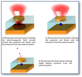
- Manufacturing of plasmonic (or photonic) nanostructures in which the nano emitters are deterministically and nondestructively placed exactly at the position for which the resonant electromagnetic field is maximum.
- Deterministic electron-beam lithography using fluorescence microscopy images
- Combination of optical and electron-beam lithography associated with fluorescence microscopy images to draw electron-beam exposure patterns. Fluorescent emitters (individual or aggregates) are imaged by fluorescence microscopy and at the same step alignment markers are created around them by means of optical lithography on a resist bi-layer covering the emitters. This bi-layer prevents the electrons of the beam from damaging the fluorescent emitters.
- Deterministically aligned optical lithography with spatially shaped laser modes
- By generating and utilizing spatially shaped laser modes like donut laser modes, the invention circumvents the problem of emitter bleaching and performs optical lithography centered over a single or aggregates of fluorescent emitters without causing any harm to the emitter.
- Automatic characterization of single emitters
- An apparatus and a software method were developed to determine the relevant parameters of the emitters (intensity distributed in wavelength, life-time and g2).
Market
- The success of advanced quantum communication relies on non-classical light sources emitting single indistinguishable photons at high flux rates and purity. Controlled positioning of nanoemitters and fabrication of nanostructures are necessary to realize such technologies.
- Conventional fabrication methods like scanning electron microscopy or optical lithography involve exposing the emitter directly and destructively to the electrons / laser of the writing beam. Two novel nondestructive manufacturing processes have been successfully developed.
Development
- Demontrator: single emitter plasmonic patch antennas with a controlled patch size and circular or elliptical shapes. TRL4
- Apparatus for automatic and simultaneous characterization of 10 sources. TRL4
IP
- Patent family « Optical Lithography» filed in 2017 (EP3583469) – EP, US, JP, CA
- Patent family « Electron Beam » filed in 2017 (EP3583468) – EP, US, JP, CA
- Software protection and know-how, filed in 2025
Valorisation strategy
- Licensing
- Startup